DC989B-A
Demonstration Circuit Board, LTC3872ETS8#TRPBF, Power Management-Voltage Regulator, Boost Converter

Need more?
| Quantity | Price |
|---|---|
| 1+ | Rs.9,822.890 |
Product Information
Product Overview
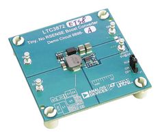
DC989B-A demonstration circuit is a single-output boost converter, it features tiny, boost controller LTC3872. The input voltage is from 3.0V to 4.5V without output de-rating. The supply has one output: 5V/2AMAX. Minimum input voltage is 2.75V. When input voltage is lower than 3V, output current should be de-rated. The design employs the LTC3872, the small footprint NO RSENSE boost regulator. The switching frequency is fixed at 550KHz. With current mode control and OPTI-LOOP compensation, DC989B-A can be optimized to provide fast transient response. NO RSENSE technique reduces both: size of the converter and power dissipation. However, care should be taken to MOSFET selection, it’s not only switching element, but also its RDS(ON) represents the current sensing element for the control loop. LTC3872 allows design small size and high efficiency step-up DC/DC solutions.
- 30mVP-P typical output ripple (VOUT) at 20MHz BW, 2A load, VIN = 3V, frequency = 550KHz
- 90% efficiency at VIN=3V, VOUT=5V IOUT=2A
Technical Specifications
Analog Devices
Power Management - Voltage Regulator
Demonstration Circuit Board LTC3872ETS8#TRPBF
-
LTC3872ETS8#TRPBF
Boost Converter
-
No SVHC (04-Feb-2026)
Technical Docs (1)
Associated Products
3 Products Found
Legislation and Environmental
Country in which last significant manufacturing process was carried outCountry of Origin:United States
Country in which last significant manufacturing process was carried out
RoHS
Product Compliance Certificate