MFS8412AMBP7ES
System Basis Chip, 2.7 V to 60 V Supply, -40 °C to 125 °C, AEC-Q100, WFHVQFN-48

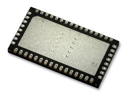
| Manufacturer | NXP |
|---|---|
| Manufacturer Part No | MFS8412AMBP7ESCopy |
| Manufacturer Standard Lead Time | 40 weeks |
| Order Code | 4784978 |
| Your Part Number | |
| Technical Datasheet |
Need more?
| Quantity | Price |
|---|---|
| 1+ | Rs.912.160 |
| 10+ | Rs.711.460 |
| 25+ | Rs.660.640 |
| 50+ | Rs.633.430 |
| 100+ | Rs.606.220 |
| 250+ | Rs.569.480 |
| 500+ | Rs.558.410 |
Product Information
| Manufacturer | NXP |
|---|---|
| Manufacturer Part No | MFS8412AMBP7ESCopy |
| Manufacturer Standard Lead Time | 40 weeks |
| Order Code | 4784978 |
| Technical Datasheet | |
| Product Range | - |
| IC Case / Package | WFHVQFN |
| No. of Pins | 48Pins |
| Supply Voltage Min | 2.7V |
| Supply Voltage Max | 60V |
| Protocol Supported | - |
| Supported Standards | ISO 26262 |
| Output Voltage | - |
| Operating Temperature Min | -40°C |
| Operating Temperature Max | 125°C |
| Qualification | AEC-Q100 |
| SVHC | No SVHC (25-Jun-2025) |
Product Overview
MFS8412AMBP7ES is a FS84 fail-safe system basis chip. It is a functionally safe, multi-output power supply IC designed for use in the automotive environment, with a specific focus on vision, ADAS domain controller, radio, and infotainment applications. It provides multiple switch modes and linear voltage regulators. The device also offers external frequency synchronization of inputs and outputs for optimized system EMC performance. It includes enhanced safety features with fail-safe outputs. The device covers the ASIL B safety-integrity level and can be fully utilized in safety-oriented system partitioning. This complies with the ISO 26262 standard and is qualified in compliance with AEC-Q100 rev H (Grade1, MSL3).
- 40V DC maximum input voltage for 12V applications
- OFF mode (power down) with very low quiescent current (10µA typ)
- 2x input pins for wake-up detection and battery voltage sensing
- Device control via 32-bit SPI interface with CRC
- BOOST converter with integrated low-side switch
- Configurable output voltage and maximum input current up to 1.5A peak
- Up to 2 linear voltage regulators for MCU IOs and ADC supply, external physical layer
- Configurable output voltage and current capability up to 400mA DC
- HVQFN48 package
- Ambient temperature (grade 1) range from -40 to 125°C
Technical Specifications
| Product Range | - |
|---|---|
| No. of Pins | 48Pins |
| Supply Voltage Max | 60V |
| Supported Standards | ISO 26262 |
| Operating Temperature Min | -40°C |
| Qualification | AEC-Q100 |
| IC Case / Package | WFHVQFN |
|---|---|
| Supply Voltage Min | 2.7V |
| Protocol Supported | - |
| Output Voltage | - |
| Operating Temperature Max | 125°C |
| SVHC | No SVHC (25-Jun-2025) |
Technical Docs (1)
Legislation and Environmental
| Country of Origin: Country in which last significant manufacturing process was carried outCountry of Origin: | China Country in which last significant manufacturing process was carried out |
|---|---|
| Tariff No: | 85381090 |
| US ECCN: | EAR99 |
| EU ECCN: | NLR |
| RoHS Compliant: | Yes RoHS |
| RoHS Phthalates Compliant: | Yes RoHS |
| SVHC: | No SVHC (25-Jun-2025) |
| Download Product Compliance Certificate | Product Compliance Certificate |
| Weight (kg): | .000001 |